

LATIF BROTHERS / PRODUCT DETAILS
The details that matter.
Review the product details below. For availability and application enquiries, contact our team or follow the external product link when provided.
Discuss your requirements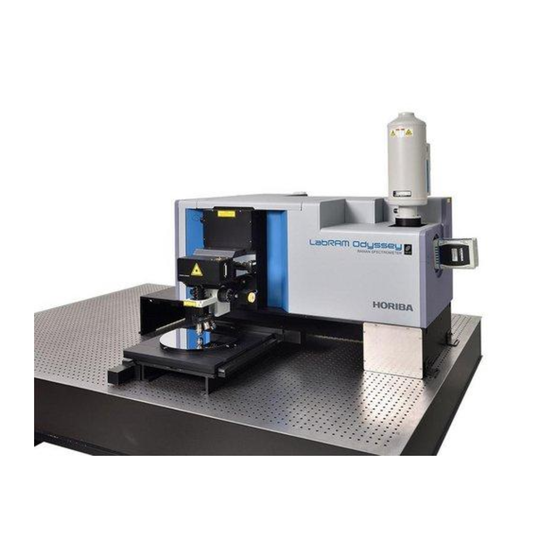
LabRAM Odyssey Semiconductor
Photoluminescence and Raman Wafer Imaging
The LabRAM Odyssey Semiconductor microscope is the ideal tool for photoluminescence and Raman imaging on wafers up to 300 mm diameter. The HORIBA best-seller true confocal microscope is equipped with automated 300 mm sample stage and objective turret to fit both needs of wafer uniformity assessment and defects inspection.
Related products
-
ZEISS Axioscope
ZEISS
Your Smart Microscope for Biomedical Routine and ResearchIn your clinical lab, such as a…
-
ZEISS Crossbeam
ZEISS
FIB-SEM for High Throughput 3D Analysis and Sample PreparationCombine imaging and analytical performance of…
-
ZEISS Axioscope for Materials
ZEISS
Microscope for Research and Routine in the Materials LabThe upright light microscope ZEISS Axioscope…
-
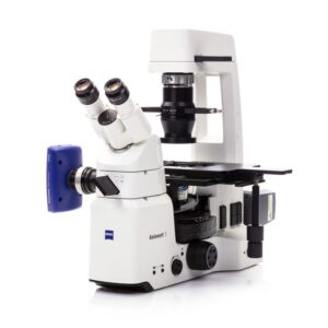
ZEISS Axiovert 5
ZEISS
Your Smart Microscope for Cell Culture and Research.Axiovert 5 brings smart microscopy into your…